CN Electronics
CN Electronics
CN Electronics
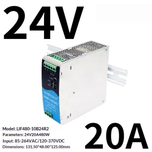
Explore our high-efficiency DIN rail power supplies, medical modules, and miniature AC/DC converters engineered for rugged operating conditions.
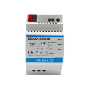
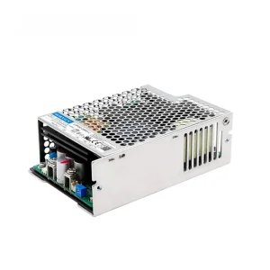
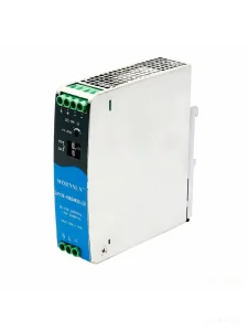
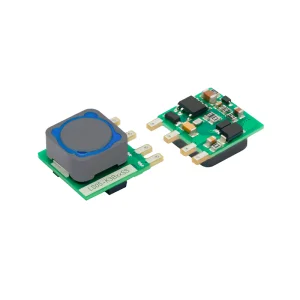
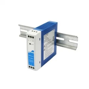
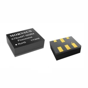
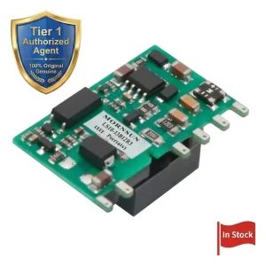
In the rapidly changing hardware ecosystem, efficiency, volume reduction, and thermal performance are the critical limiters of miniaturized electronics. Traditional inductive DC/DC converters (Buck, Boost, Buck-Boost) have served as the industry workhorses for decades. However, as medical implants, wearable technologies, IoT telemetry devices, and automotive subsystems push for structural thinning and electromagnetic silence, inductorless DC/DC charge pumps (switched-capacitor converters) have emerged as a critical architectural alternative.
CN Electronics, founded in 2006 and headquartered in the advanced manufacturing corridor of Shenzhen, China, sits at the nexus of this technological evolution. Specializing in high-precision circuit architectures, SMT layout optimization, and global OEM/ODM engineering, we support international tier-1 designers in translating charge-pump topologies from raw silicon requirements into robust, high-volume hardware deployments.
By shifting from magnetic energy storage elements (inductors) to electrostatic components (ceramic capacitors), charge pumps eliminate bulkiness, parasitic magnetic couplings, and heavy EMI shielding requirements. This makes them ideal for environments where high packing density is critical.
Integrating low-dropout (LDO) linear post-regulators or employing Pulse Frequency Modulation (PFM) allows modern custom charge pumps to maintain stable output voltages even under volatile line and load configurations, addressing traditional ripple challenges.
Optimized for remote IoT, industrial sensor arrays, and battery-powered tracking terminals, our designs minimize parasitic leakage to under 10µA, significantly extending system runtime in critical deep-sleep modes.
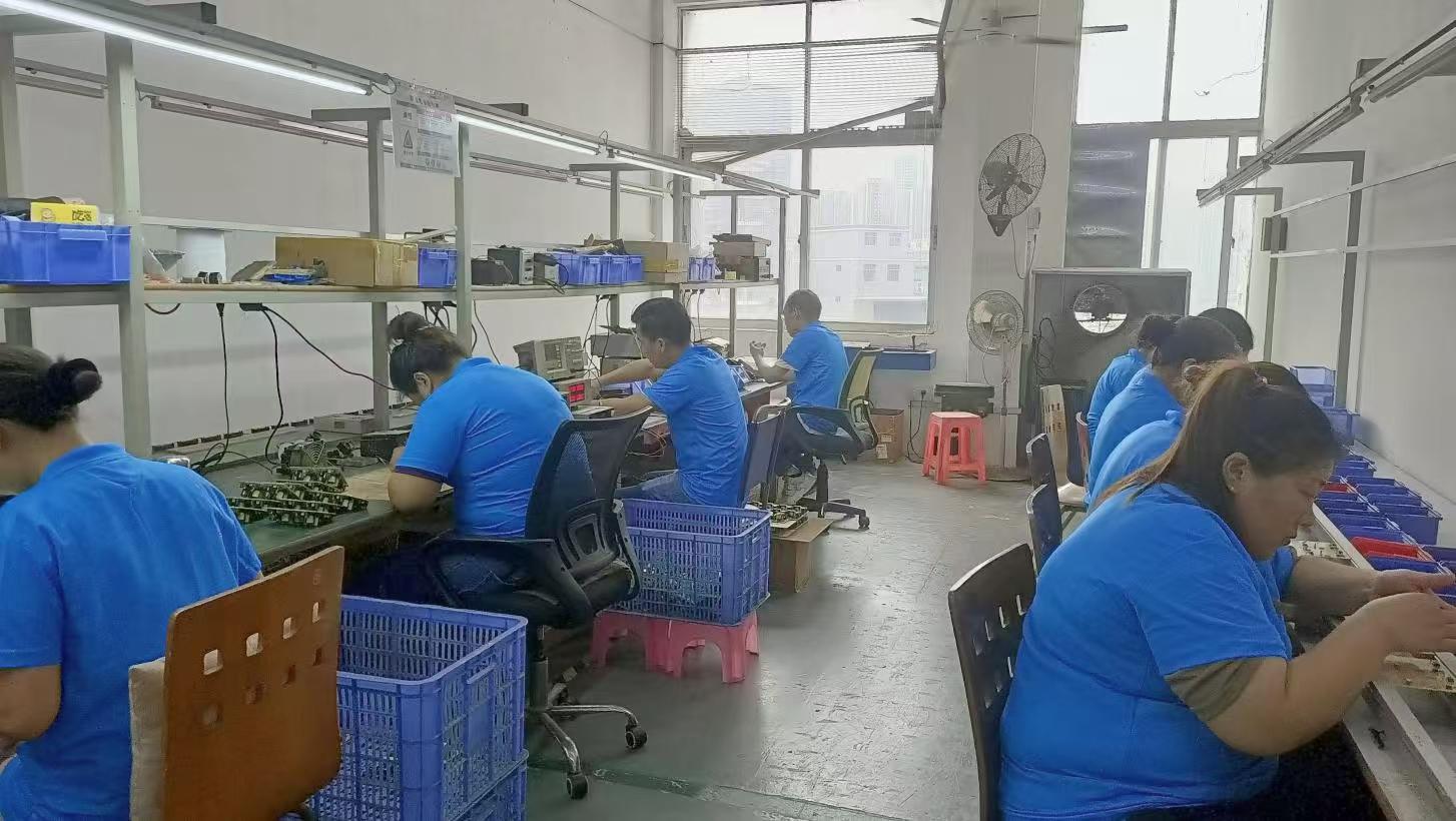
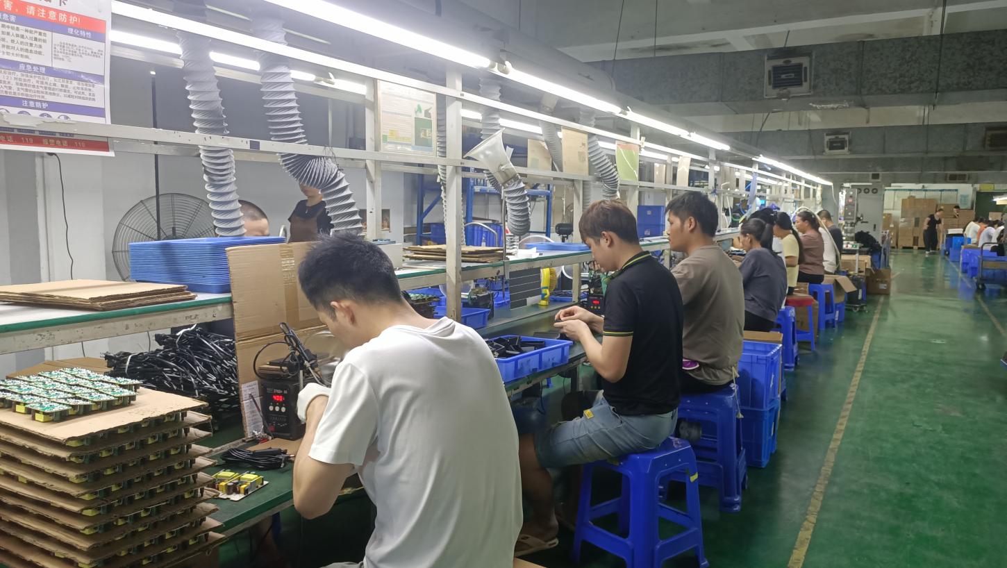
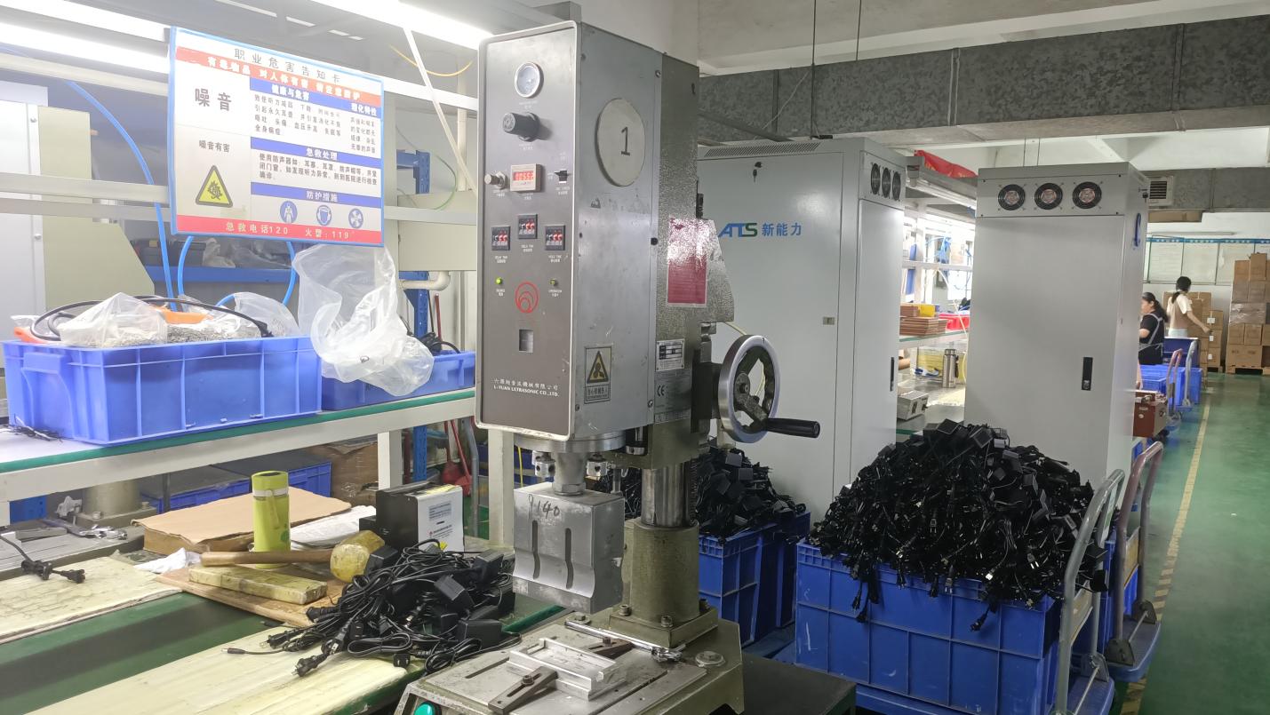
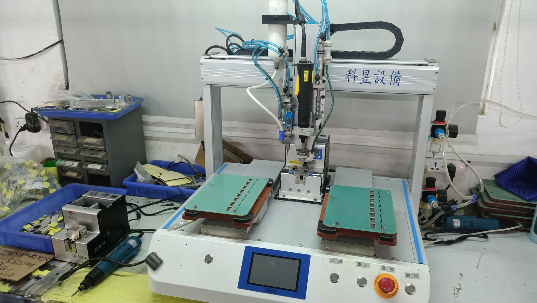
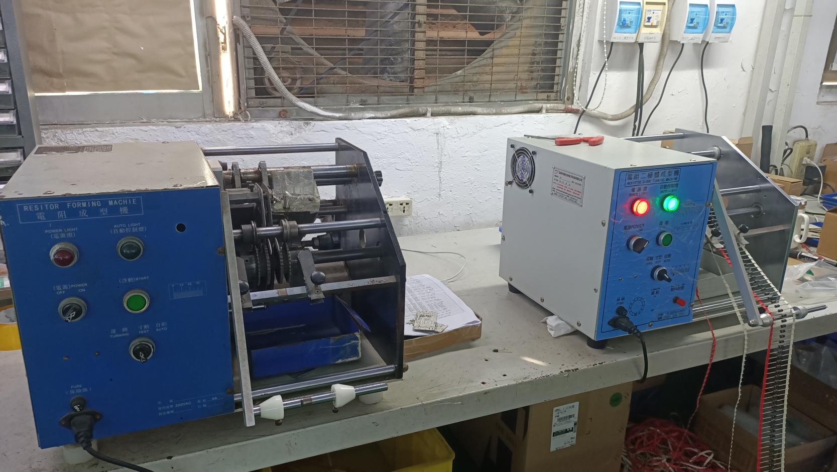
With a state-of-the-art production facility spanning over 10,000 square meters, CN Electronics integrates advanced automated assembly lines with rigorous quality control protocols. Our core capabilities cover the entire product lifecycle—including rapid PCB prototyping, component sourcing, high-volume SMT placement, and final system integration.
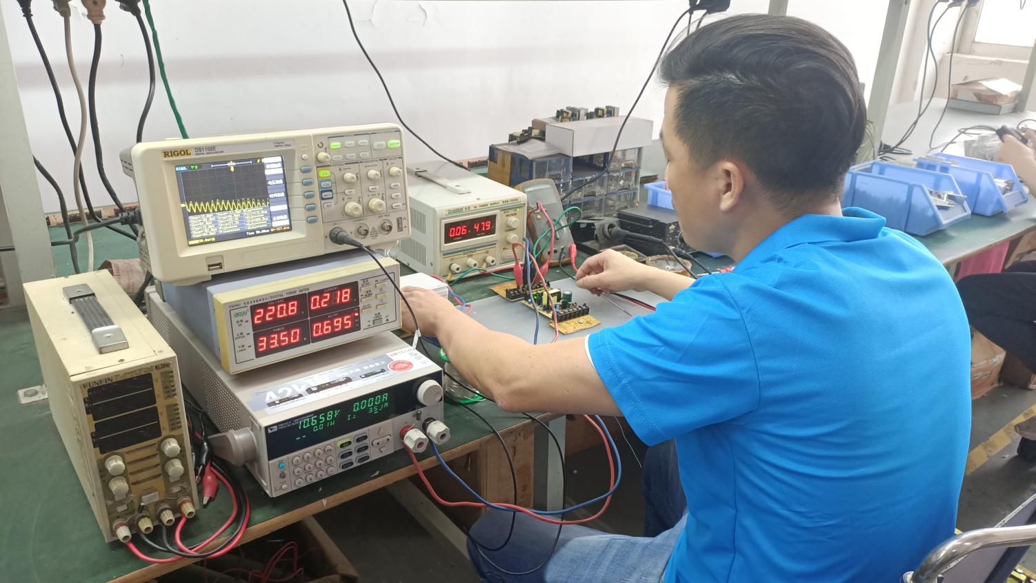
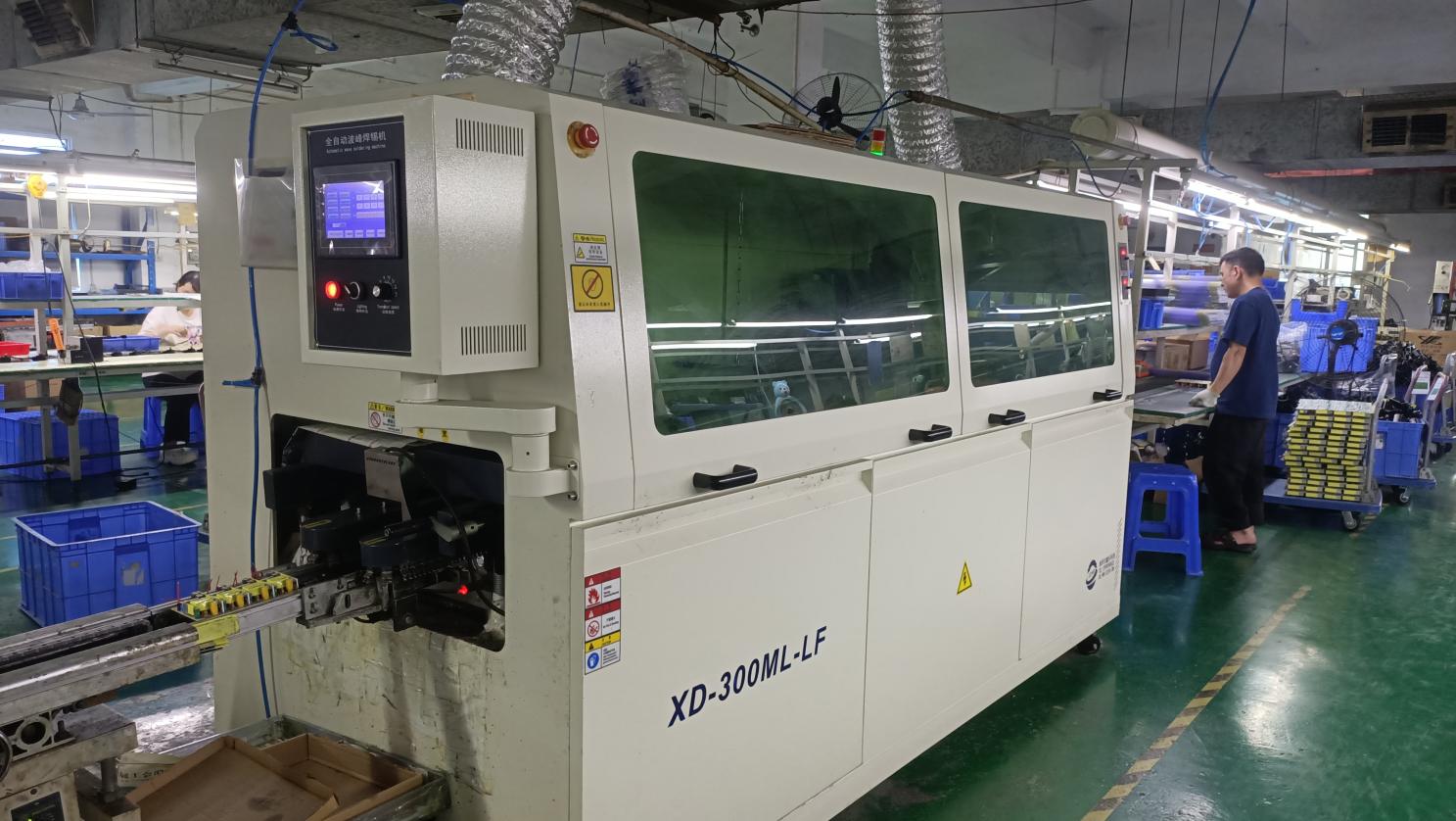
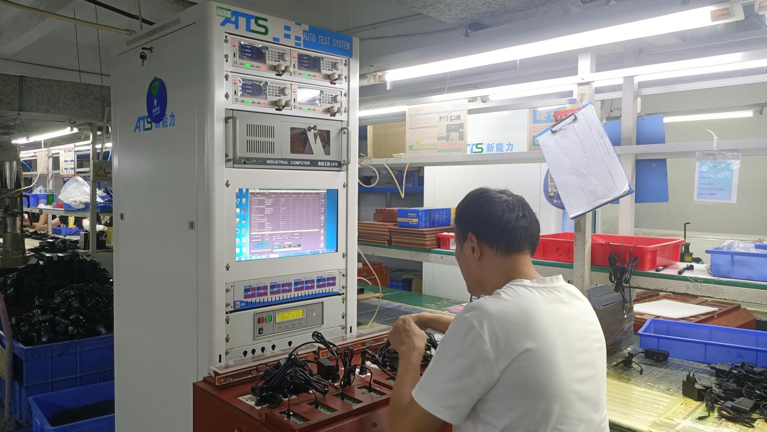
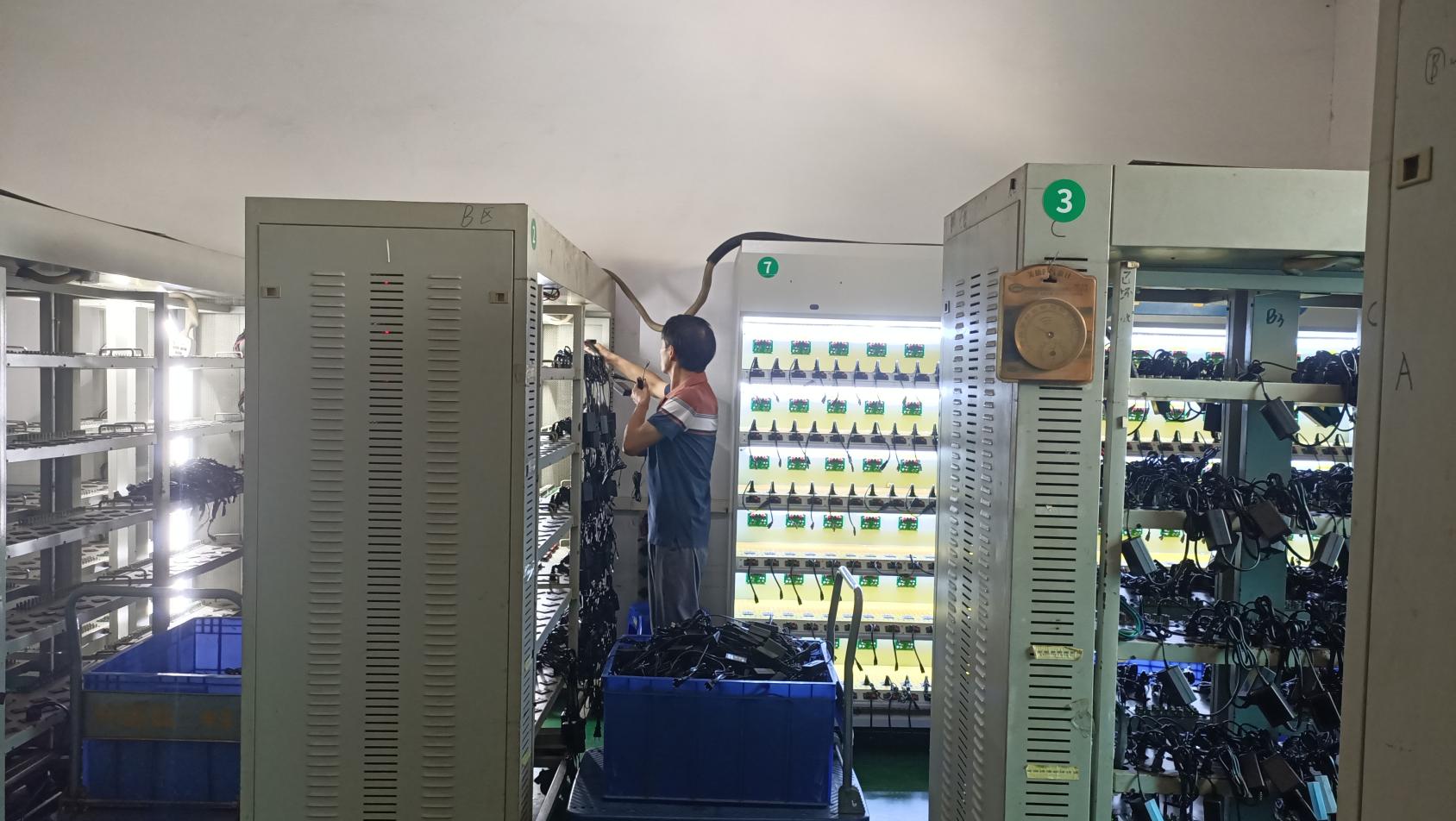
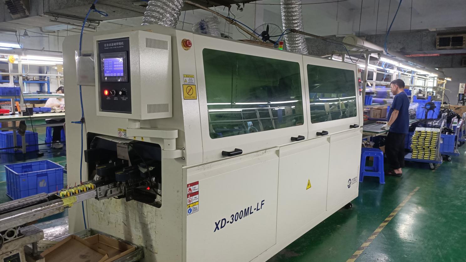
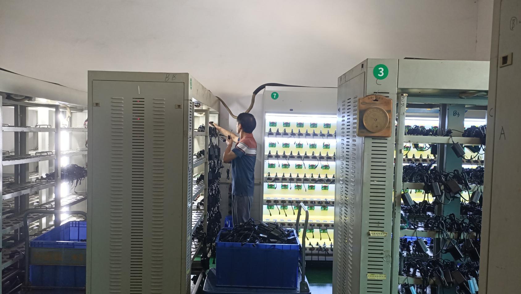
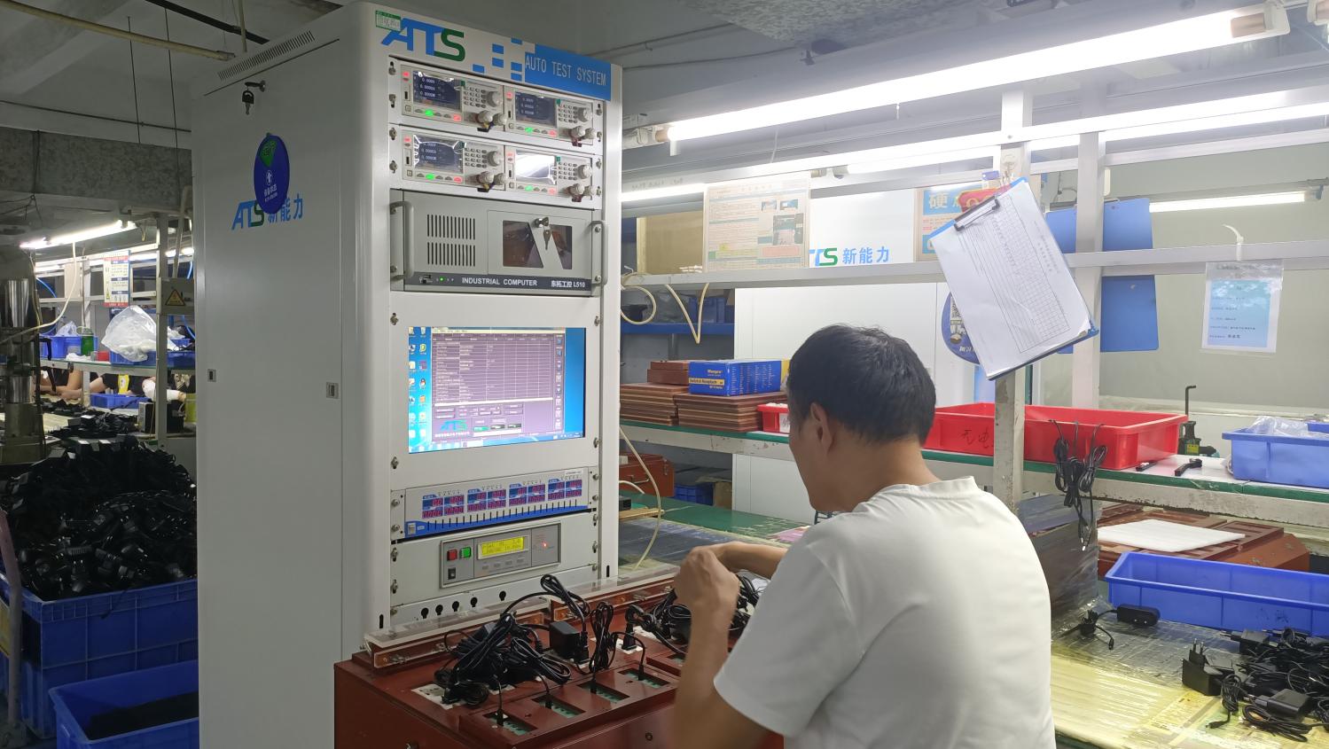
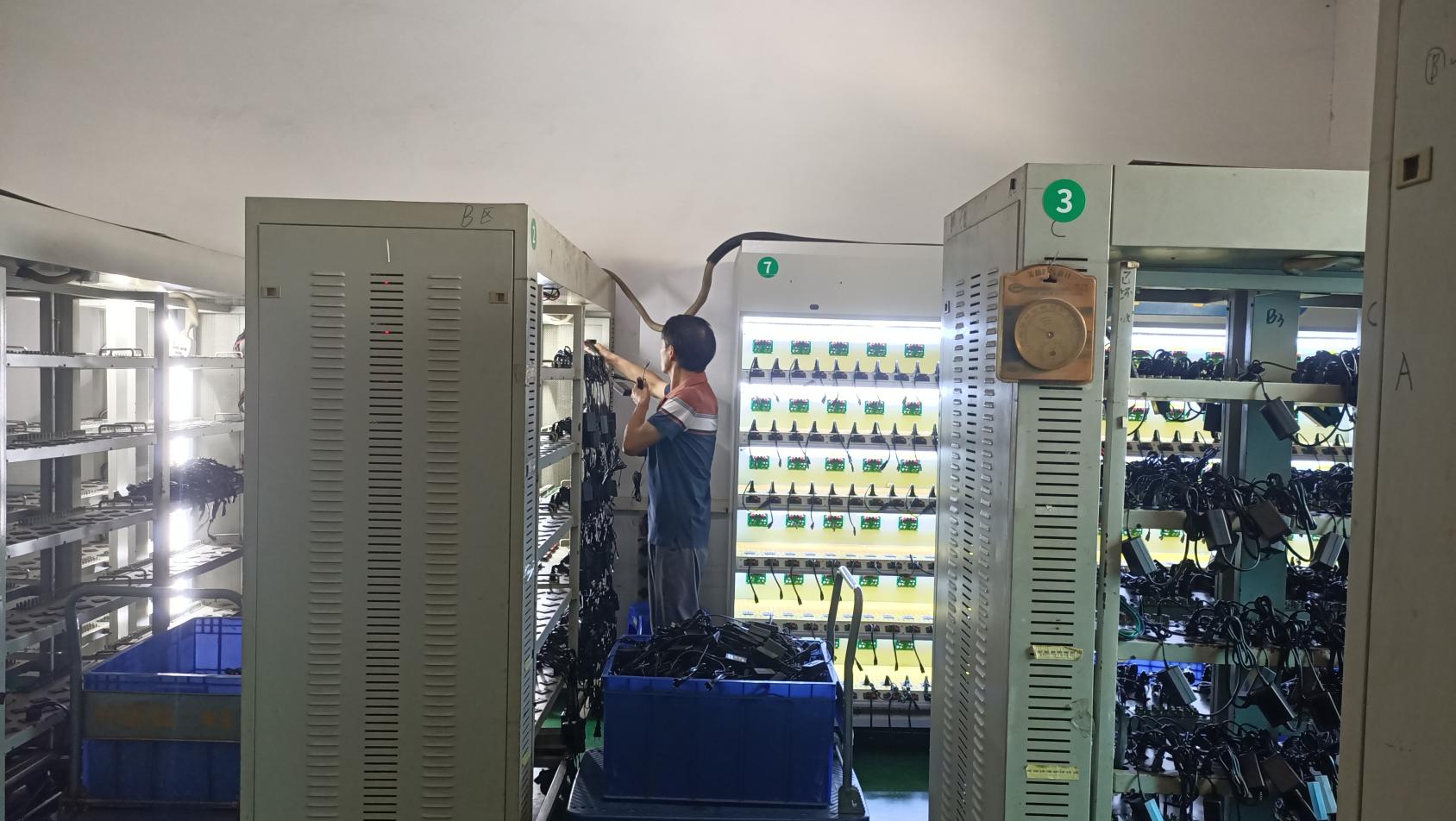
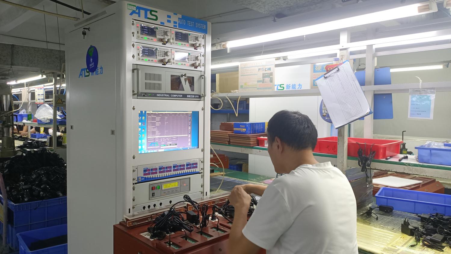
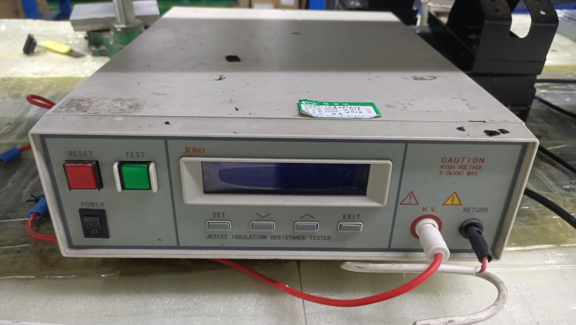
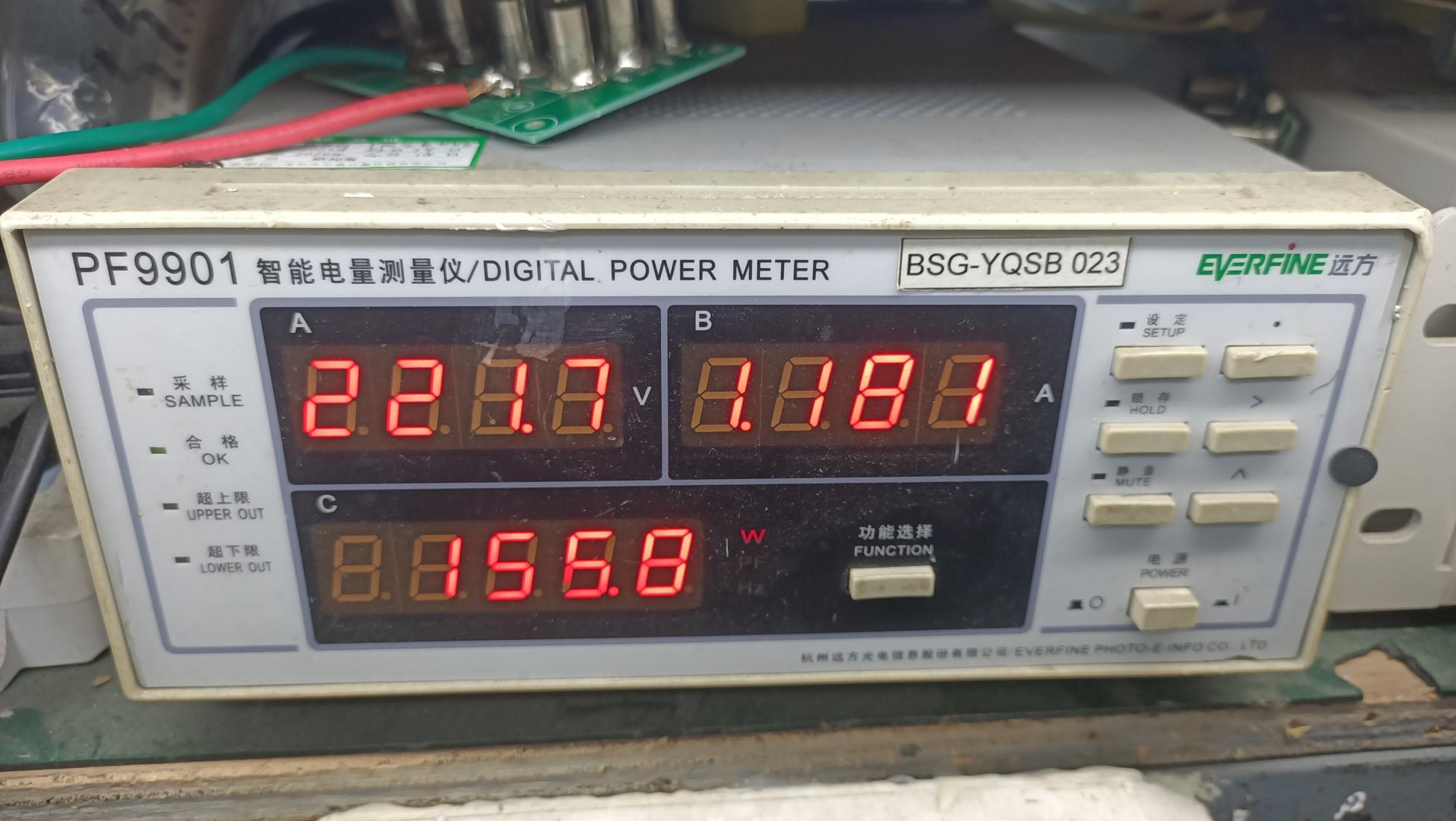
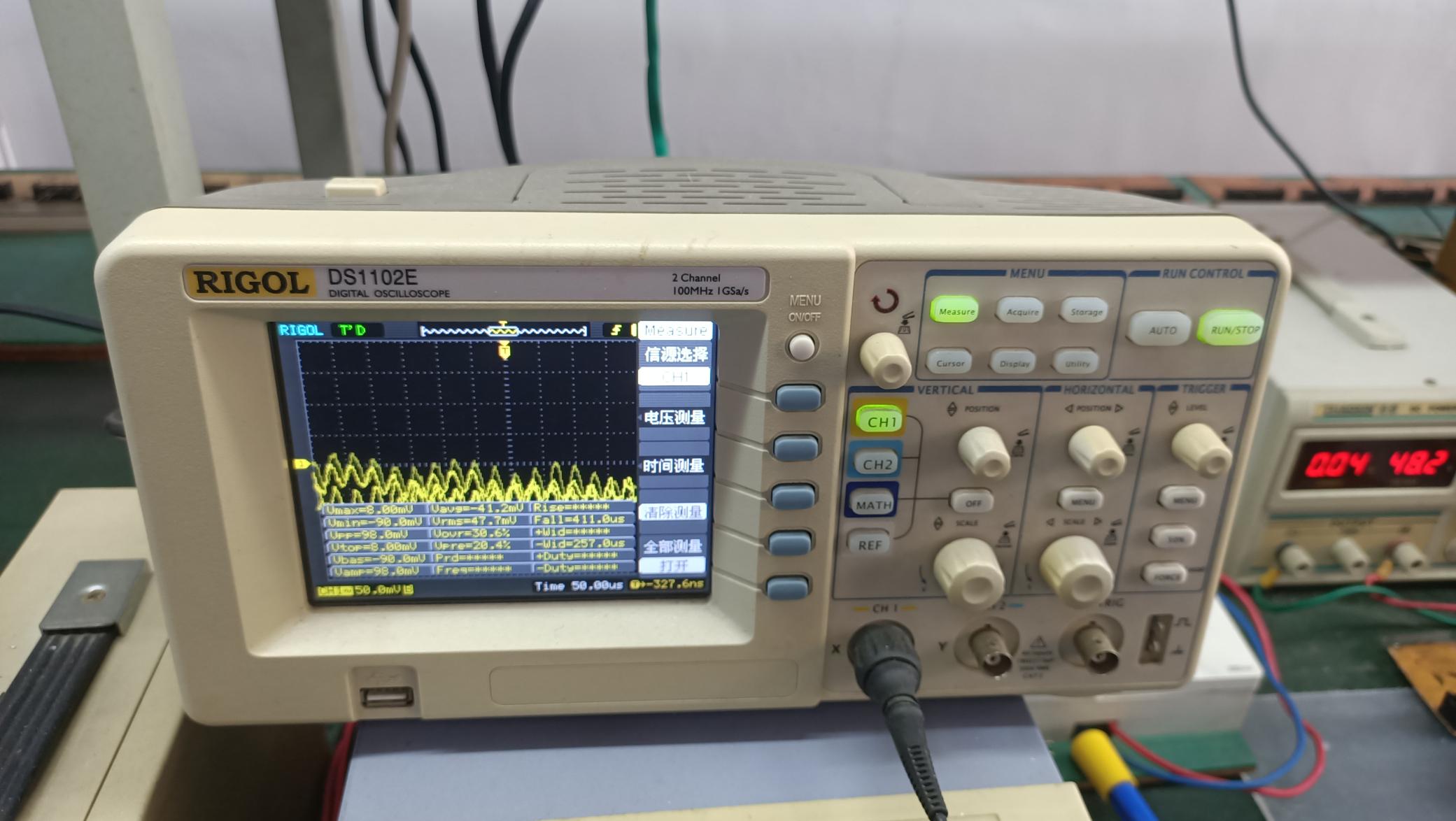
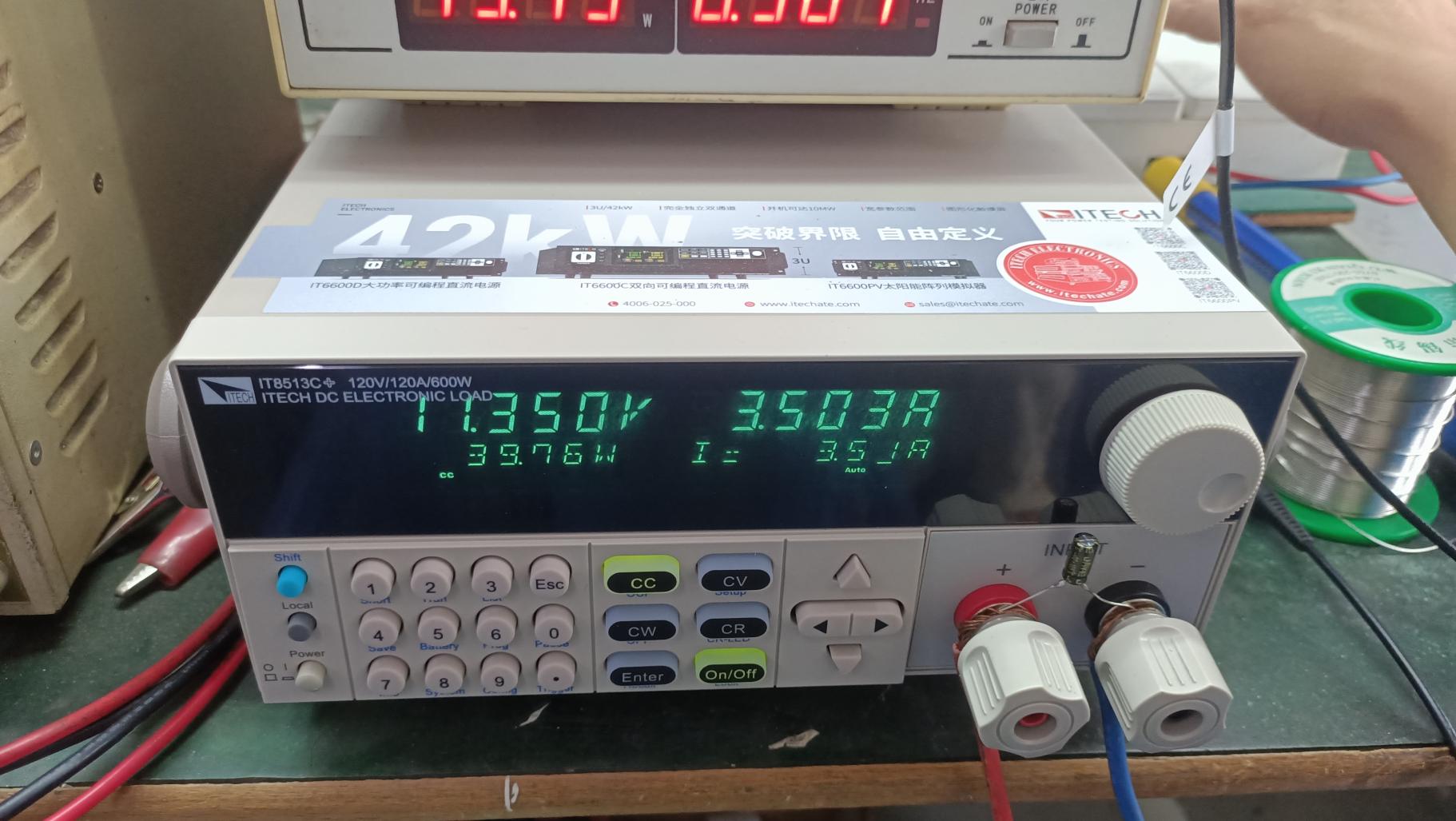
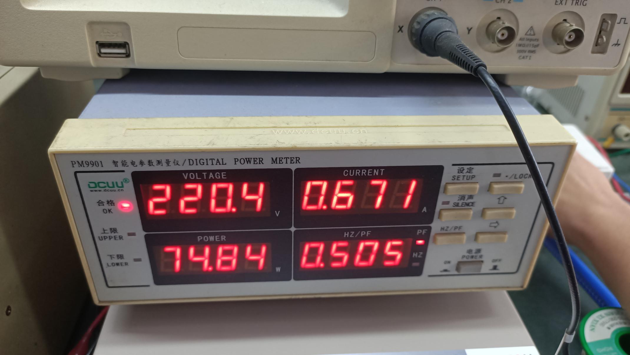
Power supplies are subjected to continuous electrical stresses, thermal fluctuations, and mechanical vibrations. At CN Electronics, we enforce strict phase-gate verification protocols. Our wave soldering machines, automatic screening devices, and high-temperature environmental aging racks guarantee that every module leaves our facility with a low field failure rate.

International electronics procurement managers frequently struggle with supply chain disruptions, uncommunicative vendors, and fluctuating raw material costs. When dealing with specialized charge pump switching circuits, finding a balance between engineering precision and mass manufacturing speed is critical. Minor mismatches in passive components (such as selecting capacitors with high ESR) can reduce output efficiency or cause overheating.
CN Electronics bridges this gap by acting as a co-development partner. We don't just execute static Gerber blueprints; we analyze bill-of-materials (BOM) configurations to find dual-source alternatives, perform thermal simulation testing, and customize packaging structures to match our client's chassis limits. Our supply chain is structured to ensure fast material sourcing and transparent manufacturing tracking.
Operating as an exporter to North America, the EU, and APAC demands absolute alignment with international regulatory standards. Power modules must comply with strict electrical safety codes, electromagnetic compatibility (EMC) regulations, and toxic chemical restriction directives. CN Electronics' products and partner components comply with CE, FCC, RoHS, ISO9001, and specialized electrical certifications:
Compliance with IEC60601-1 BF Type certifications (such as the Mornsun LOF series). This requires low leakage currents and high dielectric isolation barriers to ensure patient safety in diagnostic and clinical instrumentation.
Alignment with UL61010 and UL508 benchmarks. This ensures safe operation in high-voltage cabinets, heavy manufacturing floors, and standard 35mm DIN-Rail assemblies.
Explosion-proof certification meeting IEC60079 Zone 2 specs, preventing internal electrical sparks from triggering combustible atmospheres in petrochemical and chemical refining operations.
As the industry shifts toward higher power densities, charge pump architectures are evolving to incorporate wide-bandgap (GaN and GaAs) gate-driving circuits. These advanced materials enable switching frequencies to exceed 5 MHz, allowing engineers to use smaller flying capacitors and shrink board footprints. Below is a comparative analysis of how modern OEM charge-pump solutions stack up against traditional power topologies.
| Topology Parameters | Custom Inductorless Charge Pump | Inductive Switching Regulator | Low-Dropout Regulator (LDO) |
|---|---|---|---|
| Magnetic Component Requirement | None (Electrostatic only) | Required (Bulk Inductors) | None |
| Conversion Efficiency | High (up to 95% at fixed ratio) | High (Wide voltage ranges) | Low (Proportional to Vout/Vin) |
| EMI Signature | Extremely Low (No magnetic loop) | High (Magnetic radiation) | Negligible |
| PCB Real Estate | Ultra-Compact (Z-Height < 1mm) | Moderate to Large | Ultra-Compact |
| Application Range | Sub-10W Micro-power nodes | Up to hundreds of Kilowatts | Low-current noise-sensitive rails |
In automotive gate drivers, smart meters, and sensor telemetry units, the charge pump is often integrated directly into the ASIC or micro-board to step down bias rails or double specific sensor gate potentials. As global manufacturers shift to smaller silicon geometries, our OEM division supports the development of hybrid multi-die topologies that blend charge-pump arrays with intelligent digital voltage-tracking controllers.
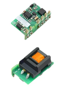
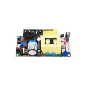
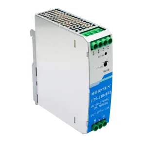
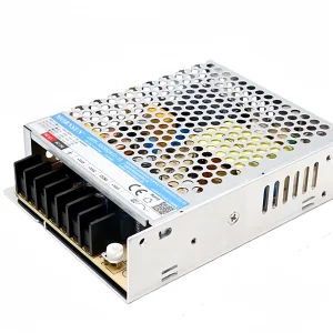
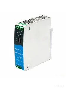
Our second tier of featured power conversion modules includes high-efficiency medical open-frame supplies, DIN-rail modules, and multi-output AC/DC converter sets.
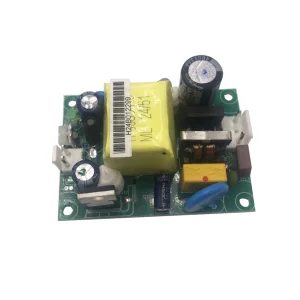
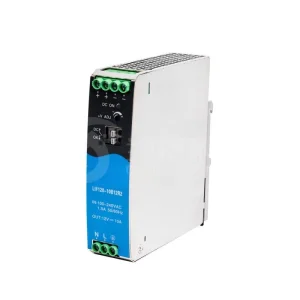
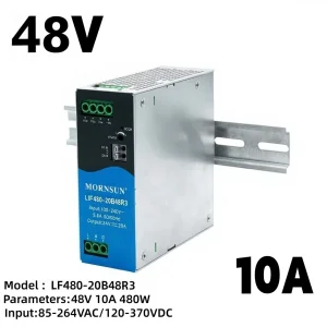
Frequently asked technical questions regarding custom designs, SMT component validations, and export logistics at CN Electronics.
The typical engineering development cycle spans 4 to 8 weeks. This timeline includes layout design, thermal simulation modeling, rapid PCB prototyping, component validation, and dynamic stress testing. For modules requiring medical-grade (IEC60601-1) or hazardous environment explosion-proof certifications, the timeline may vary depending on the target regulatory agency.
To achieve high efficiency (frequently exceeding 92%) and minimize voltage ripple, we use multi-phase flying capacitor systems, high-quality ceramic capacitors with low ESR, and low-dropout regulators (LDOs) for post-regulation. We also optimize SMT board layouts to reduce parasitic trace inductance.
Our 10,000 square meter factory is ISO9001 certified. We verify SMT alignments using Automated Optical Inspection (AOI), inspect solder joints with X-Ray systems, perform functional testing using Automated Test Equipment (ATE), and conduct high-temperature burn-in tests under full electrical load on our aging racks to prevent premature failures in the field.
Yes. We offer customization options that include modified PCB dimensions, customized structural enclosures (such as metal chassis, open-frame, or potted designs), alternative connector types, and specialized thermal configurations to fit space-constrained spaces.
We maintain long-term partnerships with leading semiconductor distributors. During our engineering review process, we identify pin-compatible components from secondary suppliers. This design flexibility helps ensure consistent manufacturing timelines even during global component shortages.